INVITATION
We look forward to seeing you at our booth.
Nanoscience and Nanotechnology Center, SANKEN, The University of Osaka
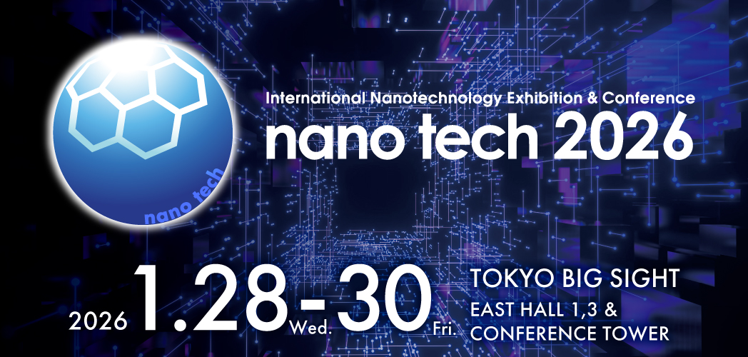
| Exhibition | : | nano tech 2026 |
|---|---|---|
| Booth | : | 1W-J28 |
| Zone | : | Innovation and Academic Zone |
| CoExhibitor(s) | : | R3 Institute for Newly-Emerging Science Design, The University of Osaka |
- Video
- Seminar
- New Product
- Demo
- Sample
- Presentation
Product / Technology Information
-
1Ionic manipulation in strongly correlated oxides: Materials and Devices
-
- Video
- Presentation
By controlling hydrogen and oxygen through electrochemistry methods, we synthesized novel strongly correlated oxides and their potential applications as memory device and thermal modulation were verified.MOVIE Product/technology Categorynano materialsNano particle, Semiconductor material, Antimicrobial material, Biocompatible materialNano Evaluation & Measurement / Analysis Technology & ToolElectron microscope (SEM / TEM), SPM / AFM, Measurement of particle size and distribution, Raman spectroscopy, High efficiency, high sensitive sensorFabrication Technology / ProcessingThin film coating (PVD・CVD), ALD・ALE, Electron beam, ion beam EUV exposure, Plasma processing, Nano imprint, Next Generation LithographyApplication FieldMaterialsFunctional hybrid material, Electric material (superconductors / dielectrics / semiconductors etc), Biocompatible material, Coating materialBiotechnologyHealth care, BiosensorSolutions
Sensing
-
2Investigation of reaction kinetics induced by ultra-short electron beams
-
- Video
- Presentation
Ultrahightime-resolutionoftime-resolvedspectroscopictechniquehasbeeninvestigated.Toachieveandtoimprovethetime-resolution,ultra-shortelectronbeamgenerationhasalsobeenstudied.Quantumbeaminducedreactionkineticshavebeenstudiedbythedirectobservationofholes,excesselectronsandradicalspecies.Utilizationofultra-shortelectronbeamisotherrecenttopicforthestudy.Theconversionofultra-shortquantumbeampulsetolightpulseenablesustogenerateTHzultra-shortlightpulseasshortattheoriginalquantumbeampulsewithperfectsynchronizationwiththequantumbeampulseandthelightpulse.MOVIE Product/technology Categorynano materialsNano particle, Semiconductor material, Antimicrobial material, Biocompatible materialNano Evaluation & Measurement / Analysis Technology & ToolElectron microscope (SEM / TEM), SPM / AFM, Measurement of particle size and distribution, Raman spectroscopy, High efficiency, high sensitive sensorFabrication Technology / ProcessingThin film coating (PVD・CVD), ALD・ALE, Electron beam, ion beam EUV exposure, Plasma processing, Nano imprint, Next Generation LithographyApplication FieldMaterialsFunctional hybrid material, Electric material (superconductors / dielectrics / semiconductors etc), Biocompatible material, Coating materialBiotechnologyHealth care, BiosensorSolutions
Sensing
-
3In situ observation of nanocatalysts under reaction environments
-
- Video
- Presentation
Using an environmental transmission electron microscope, we clarified the dynamics and atomic-scale structures of various nanoparticle catalysts, including gold, platinum, and rhodium, under reaction conditions.MOVIEProduct/technology Categorynano materialsCarbon nanotube, Nano particle, Semiconductor material, Antimicrobial materialNano Evaluation & Measurement / Analysis Technology & ToolElectron microscope (SEM / TEM), Measurement of particle size and distributionFabrication Technology / ProcessingElectron beam, ion beam EUV exposure, Plasma processingApplication FieldMaterialsCatalystAutomobileEmission control system
-
4First-principles prediction for material property and functionality
-
- Video
By solving the Kohn-Sham equation for electrons with computers, we can clarify the quantum states of materials (the electronic and phononic band structure and their density of states).MOVIEProduct/technology Categorynano materialsNano particle, Semiconductor material, Antimicrobial material, Biocompatible materialNano Evaluation & Measurement / Analysis Technology & ToolElectron microscope (SEM / TEM), SPM / AFM, Measurement of particle size and distribution, Raman spectroscopy, High efficiency, high sensitive sensorFabrication Technology / ProcessingThin film coating (PVD・CVD), ALD・ALE, Electron beam, ion beam EUV exposure, Plasma processing, Nano imprint, Next Generation LithographyApplication FieldMaterialsFunctional hybrid material, Electric material (superconductors / dielectrics / semiconductors etc), Coating material
-
5Green-Light Wavelength-Selective Organic Solar Cells for Greenhouses
-
- New Product
- Demo
- Sample
- Presentation
The development of next-generation greenhouses is increasing demand for systems that tackle energy and food challenges at once. This group is creating organic solar cells (OSCs) that use organic semiconductors as photo-active layers. Leveraging their light weight, flexibility, and wavelength selectivity, green-light-selective OSCs have been developed. They transmit blue and red light that supports plant growth while converting green light into electricity, enabling efficient solar use for both power generation and agriculture.Product/technology Categorynano materialsNano particle, Semiconductor material, Antimicrobial material, Biocompatible materialNano Evaluation & Measurement / Analysis Technology & ToolElectron microscope (SEM / TEM), SPM / AFM, Measurement of particle size and distribution, Raman spectroscopy, High efficiency, high sensitive sensorFabrication Technology / ProcessingThin film coating (PVD・CVD), ALD・ALE, Electron beam, ion beam EUV exposure, Plasma processing, Nano imprint, Next Generation LithographyApplication FieldMaterialsFunctional hybrid material, Electric material (superconductors / dielectrics / semiconductors etc), Biocompatible material, Coating materialBiotechnologyHealth care, BiosensorSolutionsSensing
-
6IoT Nanoparticle Sensors Using Artificial Intelligence
-
- Video
- Presentation
Using a single-particle detection method that combines a nanopore sensor with AI technology, we have succeeded in identifying five typical respiratory infectious viruses (coronavirus, adenovirus, respiratory syncytial virus, and influenza A and B viruses) with high accuracy.MOVIE Product/technology Categorynano materialsCarbon nanotube, Nano particle, Semiconductor material, Antimicrobial material, Biocompatible materialNano Evaluation & Measurement / Analysis Technology & ToolElectron microscope (SEM / TEM), SPM / AFM, Measurement of particle size and distribution, Raman spectroscopy, High efficiency, high sensitive sensorFabrication Technology / ProcessingThin film coating (PVD・CVD), ALD・ALE, Electron beam, ion beam EUV exposure, Plasma processing, Next Generation LithographyApplication FieldMaterialsFunctional hybrid material, Electric material (superconductors / dielectrics / semiconductors etc), Biocompatible material, Coating materialBiotechnologyHealth care, BiosensorSolutions
Sensing
-
7Support for evaluation of nanomaterials by general-purpose analytical instruments
-
- Presentation
The Nanotechnology Research Center was established in 2009 for the strategic development of nanotechnology research and the dissemination of its results. The center has introduced a group of nanodevice fabrication, structural evaluation, and functional evaluation devices, and is capable of forming nanostructures of various materials, including inorganic and organic materials, as well as analyzing and evaluating their structures, functions, and electronic properties with high precision.Product/technology Categorynano materialsNano particle, Semiconductor material, Antimicrobial material, Biocompatible materialNano Evaluation & Measurement / Analysis Technology & ToolElectron microscope (SEM / TEM), SPM / AFM, Measurement of particle size and distribution, Raman spectroscopy, High efficiency, high sensitive sensorFabrication Technology / ProcessingThin film coating (PVD・CVD), ALD・ALE, Electron beam, ion beam EUV exposure, Plasma processing, Nano imprint, Next Generation LithographyApplication FieldMaterialsFunctional hybrid material, Electric material (superconductors / dielectrics / semiconductors etc), Biocompatible material, Coating materialBiotechnologyHealth care, BiosensorSolutionsSensing
-
8Support at the Advanced Research Infrastructure for Materials and Nanotechnology Open Facilities in Osaka University
-
- Presentation
The Nanotechnology Centre at Osaka University, which participates in the Ministry of Education, Culture, Sports, Science and Technology's Advanced Research Infrastructure for Materials and Nanotechnology, provides support for microfabrication using LED, ultraviolet light and electron beam lithography techniques; support for physical properties/structure evaluation using helium ion microscopy and SPM; and various film deposition methods, such as pulsed laser MBE. In order to provide this support, the latest equipment and facilities related to nanotechnology are made available to researchers from both inside and outside the university, including those from private companies.Product/technology Categorynano materialsNano particle, Semiconductor material, Biocompatible materialNano Evaluation & Measurement / Analysis Technology & ToolElectron microscope (SEM / TEM), SPM / AFM, Measurement of particle size and distribution, Raman spectroscopy, High efficiency, high sensitive sensorFabrication Technology / ProcessingThin film coating (PVD・CVD), ALD・ALE, Electron beam, ion beam EUV exposure, Plasma processing, Nano imprint, Next Generation LithographyApplication FieldMaterialsFunctional hybrid material, Electric material (superconductors / dielectrics / semiconductors etc), Biocompatible material, Coating materialBiotechnologyHealth care, BiosensorSolutionsSensing
-
9R3:Recurrent, Reskilling and Research Retraining
-
- Presentation
R3 Institute consists of members belonging to six Graduate Schools, three Research Institutions and one Research Center, where nanoscience- and nanotechnology-related research activities are performed. It offers Recurrent and Reskilling and Retraining, characterized by advanced hands-on-practice for stimulating newly-emerging science. They are really multi-/trans-disciplinary covering physics, chemistry, biology, materials science and engineering, electronics, mechanics, medicine, etc. and become important for the sustainable development of various emerging science and technology. Experimental equipment such as Electron-beam Ultrafine Lithograph is open for joint use.science and technology.Product/technology Categorynano materialsNano particle, Semiconductor material, Antimicrobial material, Biocompatible materialNano Evaluation & Measurement / Analysis Technology & ToolElectron microscope (SEM / TEM), SPM / AFM, Measurement of particle size and distribution, Raman spectroscopy, High efficiency, high sensitive sensorFabrication Technology / ProcessingThin film coating (PVD・CVD), ALD・ALE, Electron beam, ion beam EUV exposure, Plasma processing, Nano imprint, Next Generation LithographyApplication FieldMaterialsFunctional hybrid material, Electric material (superconductors / dielectrics / semiconductors etc), Biocompatible material, Coating materialBiotechnologyHealth care, BiosensorSolutionsSensing
-
10nanotech2026 OU Booth Seminar (1W-J28)
-
- Presentation
Product/technology Categorynano materialsNano particle, Semiconductor material, Antimicrobial material, Biocompatible materialNano Evaluation & Measurement / Analysis Technology & ToolElectron microscope (SEM / TEM), SPM / AFM, Measurement of particle size and distribution, Raman spectroscopy, High efficiency, high sensitive sensorFabrication Technology / ProcessingThin film coating (PVD・CVD), ALD・ALE, Nano imprint, Next Generation LithographyApplication FieldMaterialsFunctional hybrid material, Electric material (superconductors / dielectrics / semiconductors etc), Biocompatible material, Coating materialBiotechnologyHealth care, BiosensorSolutionsSensing
Seminar Information
-
1Introduction of ARIM support cases at the Research Center for Ultra-High Voltage Electron Microscopy
-
Jan. 30, 2026 (Fri.) 15:00-15:30Pre-Registration not required
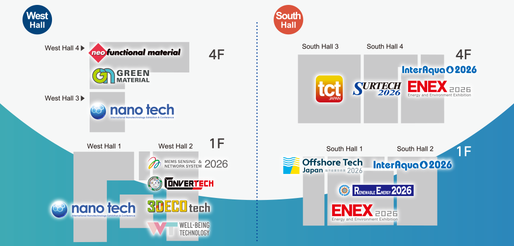
Venue : Seeds & Needs Seminar B(West hall 1) Introduction of ARIM support cases at the Research Center for Ultra-High Voltage Electron MicroscopyThe University of Osaka Research Center for Ultra-High Voltage Electron Microscopy Research Center for Ultra-High Voltage Electron Microscopy
Prof. Kaoru Mitsuoka
【Profile】The University of Osaka Research Center for Ultra-High Voltage Electron Microscopy Research Center for Ultra-High Voltage Electron Microscopy Professor
Contact
*The following information is provided to enable inquiries to exhibitors.
Unauthorized use and reproduction for any other purpose is prohibited.
| Company | : |
Nanoscience and Nanotechnology Center, SANKEN, The University of Osaka
Nanoscience and Nanotechnology Center, SANKEN, The University of Osaka |
|---|---|---|
| Address | : | 8-1, Mihogaoka, Ibaraki, Osaka 567-0047, Nanoscience and Nanotechnology Center, SANKEN, The University of Osaka, Osaka Japan 5670047 |
| TEL | : | 06-6879-8447 |
| URL | : | https://www.sanken.osaka-u.ac.jp/en/organization/#nnc |
Visitor Guidance
This exhibition is "Pre-registration required".
We kindly ask all attendees to pre-register before visiting the venue to facilitate seamless and contactless access upon entry and exit.


Access
| Venue | Tokyo Big Sight |
|---|---|
| Address (e.g. of house) | 3-11-1 Ariake, Koto-ku, Tokyo 135-0063, Japan |
| By train |
|
| Tokyo Big Sight |
Homepage: https://www.bigsight.jp/english/ Access: https://www.bigsight.jp/english/visitor/access/ |
Hall Map
The Visitor Badge is valid for All Concurrent Events.
You can share this invitation.